


Application: Precisely apply solder mask coatings to printed circuit boards
Purpose of solder resist
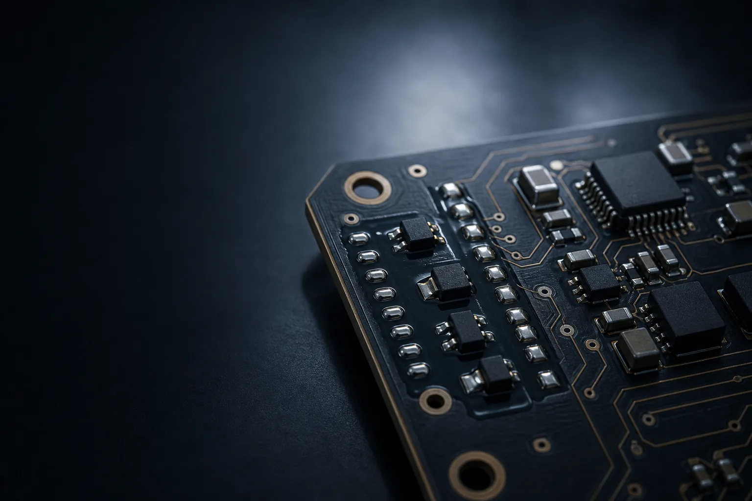
Solder resist, also known as solder mask, is a permanent protective layer on printed circuit boards. It covers conductive tracks and defined areas while leaving pads, contacts and other functional zones exposed for soldering or assembly. The layer can also provide electrical insulation and protect the board against mechanical or chemical stress.
Soldering stop paint is not equivalent to conformal coating. The soldering stop coat is typically part of circuit board production and has precisely defined recesses. Conformal Coating is later applied to the fitted assembly and protects components and circuit board against environmental influences.
When a spray application can be useful
Soldering stop paint is processed industrially with different processes. The spray application is considered where the material manufacturer releases the process and where small series, prototypes, three-dimensional geometries or difficult-to-reach areas are to be processed. Exposure, printing or other established coating processes often remain decisive for high-resolution printed circuit board structures.
Krautzberger therefore does not consider the soldering stop coating process as a whole, but rather checks whether the concrete medium and the required structure can be implemented technically meaningfully with a spray application.
Spray process requirements
The coating shall be uniform and shall not wet exposed contact areas uncontrollably. Masking, component absorption and movement guidance are therefore just as important as nozzle and material pressure.
- fine, reproducible layer distribution
- clean limitation and protection of free areas
- controlled wetting of edges and three-dimensional areas
- Avoidance of runs, pores and air inclusions
- Consideration of viscosity, solid content and pot life
- rapid cleaning for reactive or curing materials
Masking, drying and process limits
The quality of the soldering stopper not only depends on application. Before coating, printed circuit boards must be clean and dry. Depending on the material system, ventilation, pre-hardening, exposure or thermal final curing follow after application. These steps are determined by the soldering stop paint manufacturer and must be coordinated with the sprayed layer.
The masking of pads and contact surfaces is particularly relevant for a spray application. Mechanical masks or covers can be used for simple geometries. However, high-resolution structures and very small distances may require other methods. Therefore, the technical feasibility is examined in an experiment before an investment decision is taken.
- clean and dry PCB surface
- defined masking limits
- even layer before hardening
- Material compatibility with cleaning and rinsing media
- Clear delimitation to high-resolution standard procedures
Krautzberger application technology for soldering stop paint
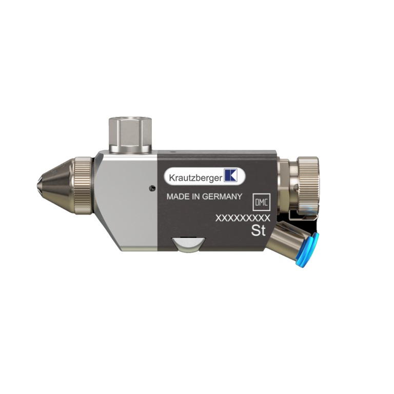
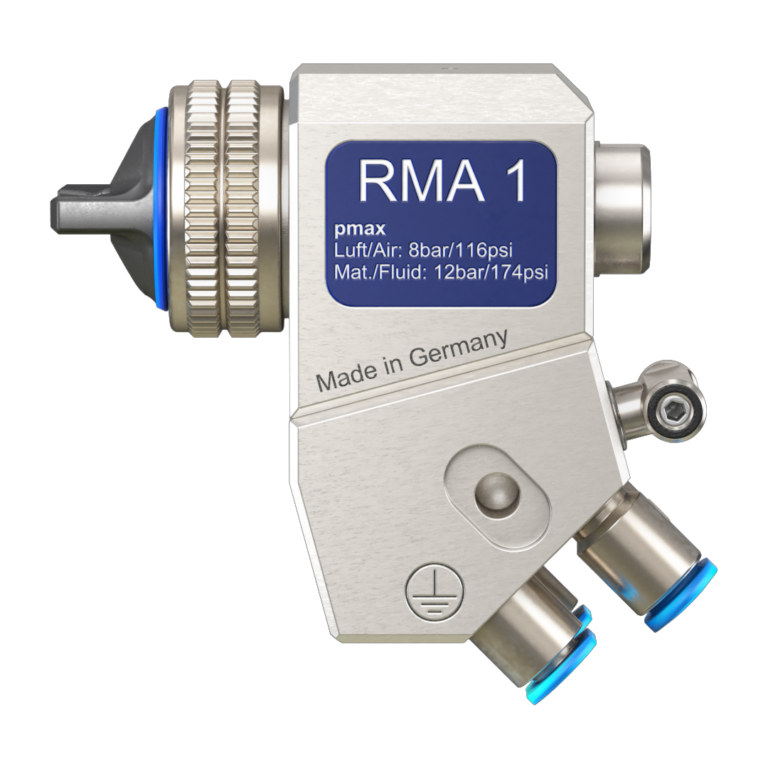
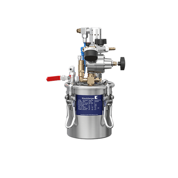
Finely adjustable manual spray guns can be used for manual samples and repair tasks. In automated processes, compact automatic spray guns enable reproducible paths and spray pulses. Material pressure vessels and precise material pressure controllers ensure a stable material flow with small application quantities.
Depending on the medium, diaphragm pumps or other delivery systems can be used. The materials of wetted components, seals and cleaning media must be compatible with the solder mask coating. With two-component systems, particular attention must be paid to pot life and dead volume.
Typical areas of application
- Prototypes and sample boards
- Small series and special formats
- three-dimensional or irregular circuit board geometries
- Targeted rework and repair
- selective protection areas outside high-resolution structures
Small quantities and frequent material changes
In prototypes and small series only small quantities of paint are often processed. A compact material container and short lines reduce residual material and simplify cleaning. At the same time, the material pressure must remain stable despite a small quantity, so that the layer from assembly to assembly does not change.
Separate material paths or a thoroughly validated flushing are required for changing soldering stop coats or paints. Residues of a previous system may affect curing, hue or adhesion.
- Short material paths
- Low dead volume
- constant pressure at low flow rate
- safe separation of different paint systems
- defined cleaning before material change
Process tests and validation
Soldering stop coatings differ significantly in viscosity, pigmentation, reactivity and hardening. Original material and sample conductor plate can be tested in the Krautzberger technical test centre. Sprayability, layer distribution, edge cover, masking and cleaning behaviour are evaluated.
The electrical function, curing and fulfilment of the requirements applicable to the printed circuit board must then be validated by the operator or PCB manufacturer.
Advantages of a coordinated spray solution
- flexible application on prototypes and special geometries
- finely adjustable quantity of material
- manual and automatic process variants
- coordinated material supply for small quantities
- Tests with original material prior to the plant decision
Related products
All products

Suitable solution for your soldering stop paint
Are you looking for a fine spray gun, an automatic spray gun or a material supply for soldering stop paint or soldering protection varnish? Krautzberger is working with you to check whether and how the concrete material can be sprayed.
Talk to us about paint system, PCB geometry, masking, layer thickness and quantity.
Industries for this application
Soldering stop paint protects conductors, while pads and contacts remain free for later soldering and assembly steps. In PCB production, the spray application must therefore distinguish between a closed protective layer and precisely defined recesses.
